PCBA
Reliable PCB Assembly,
From Quote to Delivery
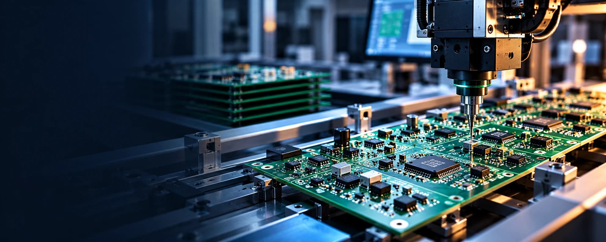
From prototype builds to production requirements, AEMS provides end-to-end PCBA services including component sourcing, SMT and through-hole assembly, inspection, and testing. Upload your design files and requirements — our engineering team reviews your job, prepares the quotation, and manages the assembly process through completion and delivery.
- Quoted by an engineerRead from your Gerbers and BOM
- Inspected three timesSPI, AOI and X-ray on the line
- SMT & through-holeAssembly, sourcing and testing
- 4–7 daysWorking days, to dispatch
What we do
Everything an assembly needs, in one place
Engineering, sourcing, assembly, inspection and testing — quoted together, tracked together.
Engineering
- DFM
- Design review
- Support
Manufacturability checks on your files before anything is built, and an engineer to talk to throughout.
Component Sourcing
- BOM review
- Components
- Availability
Every BOM line matched to a real part, with alternates proposed for your approval when stock runs short.
PCB Assembly
- SMT
- THT
- Mixed
Surface-mount and through-hole assembly, on one side or both, from your BOM and pick-and-place file.
Quality Checks
- SPI
- AOI
- X-ray
Paste inspected before the parts go on, the joints after, and X-ray for the ones no camera can see.
Testing
- Electrical
- Functional
Electrical tests on the assembled board, and functional tests run to your own procedure.
Production
- Prototype
- Small batch
- Production
From the first few boards to production runs, on the same files and the same process.
Packing
- Antistatic
- ESD
- Cardboard
Boards packed the way they have to travel, and labelled for the line that receives them.
On the assembly line
Every stage has a purpose.
Follow the board from solder paste to inspection. Each station prepares it for the next.
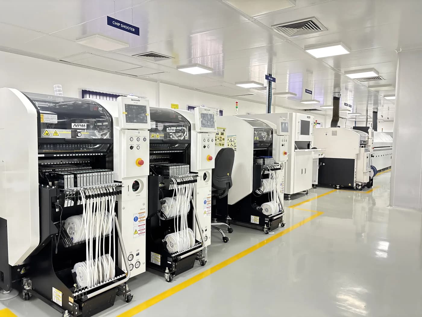
- 01
Magazine loader
PCB loading & preparation
- 02
Stencil printer
Solder paste printing
- 03
SPI
Automated solder paste inspection (SPI)
- 04
Pick & place
High-speed component placement
- 05
Reflow oven
Reflow soldering
- 06
AOI
Automated optical inspection (AOI)
- 07
X-ray
X-ray inspection
- 08
Inspection & packing
Final quality inspection & packaging
Capabilities
PCBA capabilities
What the line places, how it is inspected and how it leaves us. Need something not listed? Ask our engineers.
Assembly
SMT, THT & mixed-technology assembly
Our production capabilities support surface-mount, through-hole, and combined assembly requirements for prototype builds as well as production quantities.
Single- & double-sided PCB assembly
Assembly can be performed on both sides of the PCB, supporting a wide range of board designs and component configurations.
Fine-pitch & high-density component assembly
Capable of handling miniature components such as 01005 and 0201, along with advanced packages including QFN, QFP, BGA, and LGA.
Advanced soldering processes
Nitrogen reflow soldering for improved solder joint quality and process consistency, plus wave and selective soldering for through-hole components and assemblies requiring controlled solder application.
Testing & inspection
Solder paste inspection (SPI)
2D/3D inspection technology is used to evaluate solder paste deposition and identify printing-related issues such as insufficient paste, excess paste, offset, and bridging.
Automated optical inspection (AOI)
Automated inspection helps identify visible assembly issues including missing components, incorrect placement, polarity errors, and soldering defects.
X-ray inspection
X-ray inspection enables examination of concealed solder joints and internal connections, particularly for packages such as BGA, QFN, and LGA.
Functional testing
Boards can undergo power-on and functional checks based on the customer's testing requirements to verify operation before shipment.
Process control & supporting equipment
Automated solder paste management system
Automated control helps maintain consistent solder paste condition during production while supporting process monitoring and traceability.
Precision stencil cleaning machine
Dedicated stencil cleaning equipment helps maintain printing quality by keeping the stencil surface clean and preserving consistent paste deposition.
SMT machinery & equipment
Every station a board passes, in order.
- Magazine loaderPCB loading & preparation01
- Stencil printerSolder paste printing02
- SPIAutomated solder paste inspection (SPI)03
- Pick & placeHigh-speed component placement04
- Reflow ovenReflow soldering05
- AOIAutomated optical inspection (AOI)06
- X-rayX-ray inspection07
- Inspection & packingFinal quality inspection & packaging08
Assembly
What goes on the board, and where.
- Assembly type
- SMT · Through-hole · Both
- Assembly side
- Top · Bottom · Both sides
- Board envelope
- Up to 500 × 400 mm
- Copper layers
- 1, 2, 4, 6 layers
- Component sourcing
- By AEMS · By you · Mixed
- Stencil
- Made by AEMS, or supplied by you — and stored here for repeat orders
Soldering
The paste, the profile and the atmosphere.
- Solder alloy
- Lead-free (RoHS) · Leaded (SnPb)
- Solder paste
- High temperature · Medium temperature
- Nitrogen reflow
- Available on request
- Build standard
- Class 2, standard · Class 3, high reliability
Inspection & test
Three looks on the line, then the tests you ask for.
- On the line
- SPI before reflow · AOI after · X-ray for hidden joints
- Electrical
- Continuity and isolation on the assembled board
- Functional
- Run to your own procedure, on your own fixture
- First article
- One board built, inspected and signed off before the batch
Finishing & delivery
How the board is protected and how it travels.
- Board cleaning
- Available on request
- Conformal coating
- Top · Bottom · Both sides, in acrylic, urethane, silicone
- Packing
- Antistatic bubble sheet · ESD packaging · Cardboard
- Lead time
- 7 working days, express 4
Design files
Files that build right the first time
What our engineers look for when they review a board.
Gerbers as one ZIP
Every Gerber layer and the drill file in one ZIP. Layer names from KiCad, Altium, Eagle and EasyEDA are recognised.
A BOM with designators
Designator, quantity, value, footprint and a manufacturer part number on each line, with do-not-populate parts clearly marked.
A placement file
X and Y position, rotation and side for every part, in the same units as the board.
A board we can make
An outline on its own layer, and up to eight layers. Fine traces and small drills are checked by an engineer before quoting.
The process
How our PCBA process works
- 01
Upload your files
Submit your Gerber files, BOM, Pick & Place/XY data, schematic, assembly drawing, and project requirements.
- 02
Request a quote
Raise your PCBA quotation request through the AEMS platform.
- 03
Engineering review
Our engineers review your submitted files, BOM, specifications, quantity, and assembly requirements.
- 04
Quotation confirmation
AEMS evaluates the job and provides the confirmed quotation.
- 05
Accept the quotation
Review the quotation and confirm your order.
- 06
Make payment
Complete the required payment to proceed with the job.
- 07
Send materials
Send the required PCB materials and components to the AEMS facility as per the agreed requirements.
- 08
Material verification
Our team receives and verifies the materials and confirms the received material details with you.
- 09
Customer confirmation
The job proceeds after the customer confirms the material verification.
- 10
Job starts
PCBA assembly begins according to the approved requirements.
- 11
Job completed
The assembled PCBs undergo the agreed inspection and testing process.
- 12
Packing & delivery
Completed assemblies are packed securely and dispatched for delivery.
FAQ
Questions, answered
Why isn't there an instant price?
Which files do you need?
Can I supply some components myself?
Which design tools do you accept?
Your next project
Ready to build your boards?
Send your design files — our engineering team reviews them and prepares a quotation.